 Product Center

Focusing on ultra-high-speed, high-speed high-precision data converters, clock signal conditioning chips, RF transceivers and system solutions.
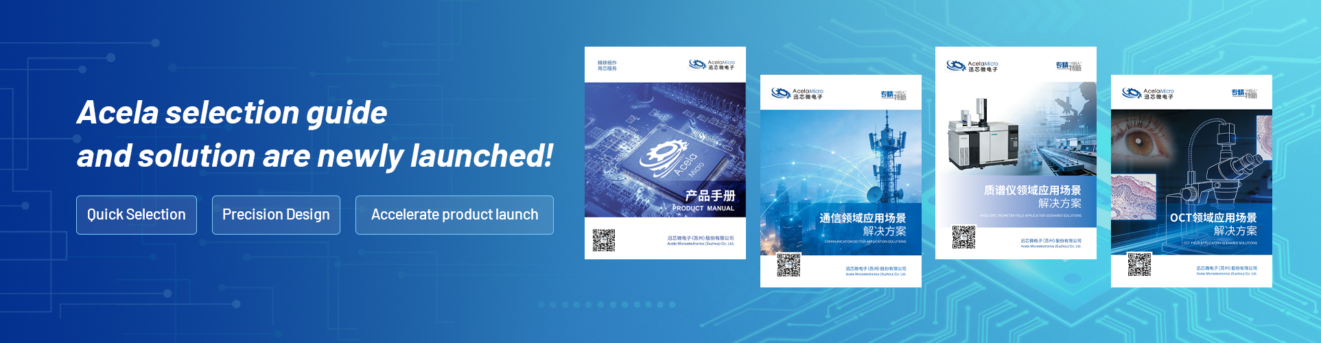
Comprehensive product portfolio covering test and measurement, communications, industrial, medical and many other fields.
Committed to independent R&D of high-end signal chain products, localization of high-performance data conversion chips, and provision of cost-effective customized chip solutions and comprehensive system services.
Providing comprehensive system solutions.
AcelaMicro's product portfolio, including variable gain amplifiers (VGAs), sample-and-hold chips, ADCs, PLLs, clock distribution chips, and high-speed comparators, can be applied in signal conditioning, sampling circuits, clock synchronization circuits, and trigger circuits. We provide a full range of analog chipset solutions for domestic high-end, mid-range, and entry-level oscilloscopes.
Based on AcelaMicro's ultra-high-speed and wide-bandwidth ADCs, DACs and clock distribution chips, we support coherent optical communication, laser communication, 6G communication, millimeter-wave communication, broadband wireless communication and other fields. We deliver real-time acquisition and waveform generation of high-speed broadband analog signals, and provide customers with algorithm and SoC verification services.
Based on our high-speed and high-precision ADCs, high-accuracy ADCs, signal conditioning chips, clock link chips and other semiconductor products, AcelaMicro provides high-speed and high-precision data acquisition boards for OCT systems, mass spectrometers, optical fiber sensing detectors, large scientific installations, CT equipment, ultrasound devices, dedicated ATE test machines and other application scenarios.
About Us


 News Center
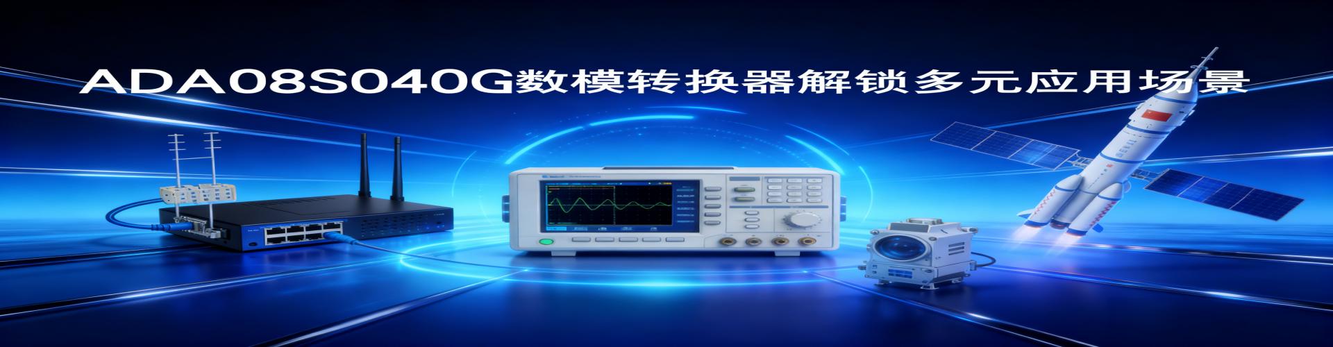
Cross-domain Empowerment | Acela Micro ADA08S040G DAC Unlocks Diverse Application Scenarios
ADA08S040G Digital-to-Analog Converter Cross-domain Empowerment, Unlock Diverse Application Scenarios Key highlight: What makes this DAC stand out from the crowd? Acela Micro ADA08S040G is a single-channel non-interpolating high-speed digital-to-analog converter fabricated with advanced CMOS process. It delivers a maximum sampling rate of 40 Gsps. Incorporating cutting-edge chip design technologies, it achieves comprehensive breakthroughs in core indicators including sampling rate, signal accuracy and interface compatibility, redefining the performance benchmark for high-speed DACs. As a critical component bridging digital and analog signals, it acts as a high-precision "signal interpreter", efficiently converting binary digital codes into continuous and stable analog signals. It provides solid support for efficient equipment operation and fully meets the stringent signal conversion requirements of high-end electronic systems.


The relocation and ribbon-cutting ceremony for the upgraded mass production laboratory of Acela Micro was successfully held!
Expanding production and upgrading, forging ahead toward our vision. In response to market demands, strengthen the quality control system and consolidate mass production and R&D capabilities, the ribbon-cutting ceremony for the upgraded and relocated mass production laboratory of Acela Micro grandly kicked off at the new site on March 18th. Company leaders, core backbones and representatives of the R&D team gathered together to celebrate the opening of the new premises and witness a crucial milestone of Acela Micro in the field of mass production.
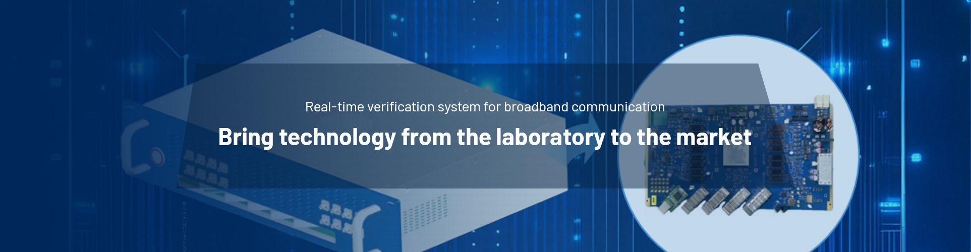
Acela Micro Breaks Through Bottlenecks in Optical Communication Validation!
AUV1302 Wideband Real-Time Validation Platform: Enabling Technologies to Move from the Laboratory to the Market 01 Solve Industry Pain Points, Empower Industrial Upgrading The iterative upgrading of optical communication technologies serves as one of the core driving forces for the development of the digital economy. A complete closed loop of theoretical design – real-time validation – engineering implementation is the key to translating technologies from laboratory research to industrial application. For a long time, the R&D of cutting-edge optical communication technologies has long been trapped in the dilemma of "excellent theoretical simulation yet hindered engineering deployment", with insufficient sampling rate and bandwidth of ADC/DAC devices acting as the core bottleneck of the industry. Today, the AUV1302 high-performance real-time validation platform for optical communications features high-spec modules with a 40 GSps sampling rate, 18 GHz bandwidth and a powerful computing core. It accurately addresses industry pain points, acts as a core engine to drive Optical Communication Technologyfrom the laboratory to the market, and delivers a series of world-leading technological achievements. 02 Robust Architecture, Empowered Validation Capabilities The AUV1302 is a high-performance, modular and programmable real-time data processing platform. It deeply integrates ultra-high-speed data acquisition and waveform generation functions, and is fully tailored for high-end optical communication validation requirements in terms of hardware architecture and functional design. The platform adopts a flexible daughter-card and mother-card architecture, enabling free daughter-card configuration for different application scenarios to deliver customized verification solutions. The high-performance data acquisition and generation daughter-card is equipped with Acela Micro 40 GSps 8-bit ADC chip AAD08S040G and DAC chip ADA08S040G, which perfectly supports real-time acquisition and generation of high-speed and broadband analog signals. The data processing mother-card integrates a large-scale FPGA, together with abundant peripheral interfaces including high-speed optical module ports and network ports, delivering powerful computing power for real-time processing of massive data.In terms of core acquisition and playback performance, the platform supports up to 4-channel synchronous sampling at 40 GSps via ADC, or 4-channel synchronous signal playback at 40 GSps via DAC, easily meeting the processing requirements of ultra-high-speed optical communication signals. Meanwhile, the system is built with an independent clock generation unit to support standalone operation without an external clock. A reserved external reference clock interface is also provided for flexible clock source configuration, adapting to multi-scenario verification demands. 微信图片_20260317102538 03 Extreme Parameters, Maximize Verification Capabilities As a benchmark platform for real-time optical communication validation, the AUV1302 features comprehensive technical specifications covering processors, interfaces, storage, clocks and other dimensions. Every parameter demonstrates powerful hardware performance, delivering ultimate support for technical validation: Powerful Computing Core It is onboard with a large-scale FPGA, featuring over 3700K logic resources, more than 80 Mb Block RAM, over 12,000 DSP units, and more than 120 high-speed SerDes interfaces, enabling real-time processing of high-speed and massive data. Rich High-Speed Interfaces ✅ 4 QSFP28 connectors with native hardware support for 100Gbps ultra-high speed; ✅Ethernet interface equipped with W5300 bridge chip, fully compatible with TCP/IP protocols; ✅ Dedicated JTAG interface supports FPGA secondary development and program solidification, meeting personalized R&D requirements. Stable Storage and Clock System ✅ 1Gbit QSPI Flash memory + 64Kbit EEPROM to meet dual demands of data storage and program operation; ✅ Built-in system reference clock source with fine frequency offset trimming; precise system clock distribution realized via PLL. ✅ Reserved with 10-channel 3.3V FPGA IO interfaces, 6 LVDS interfaces and 5 pairs of 25Gbps SMPM transceivers, delivering excellent scalability. Convenient Supporting Software It provides complete ADC and DAC drivers, along with visualized upper-computer DEMO software, greatly lowering the development threshold, enabling researchers to get started quickly and improving verification efficiency. 04 Application Topology, Adaptable to Multi-domain Scenarios Boasting core characteristics of high performance, modularity and programmability, the AUV1302 platform delivers in-depth coverage of application scenarios in optical communication and related high-end technological fields, serving as an all-purpose foundation for technological R&D and product verification. 四收四发 ✅ Broadband Optical Communication: supports the verification of cutting-edge technologies such as 200G-class high-speed transmission,high-sensitivity receivers, and broadband bidirectional systems; ✅ Broadband Wireless Communication: meets the requirements for acquisition, processing and simulation verification of ultra-high-speed wireless signals; ✅ High-performance ASIC Prototyping: Provides real-time data processing and functional verification support for chip prototype design. 05 Core Value: Breaking Theoretical Barriers As a benchmark real-time verification platform for optical communication, the AUV1302 bridges the gap between theory and engineering. It delivers full-scenario verification support featuring testability, optimizability and practical implementability for cutting-edge technologies.Covering scenarios ranging from 200G-class high-speed transmission and flexible rate adaptation to high-sensitivity receivers and broadband bidirectional systems, the platform empowers the implementation of all technical outcomes with robust capabilities in signal acquisition, real-time processing and scenario simulation. It enables comprehensive performance refinement and cost optimization at the technical verification stage. In the future, as optical communication technology evolves toward higher speeds, broader compatibility and lower power consumption, the core role of real-time verification platforms will become increasingly prominent.Continuously upgraded and iterated, the AUV1302 will adopt optimized configurations in bandwidth, sampling rate and computing power to cover more cutting-edge technology verification scenarios. It will deliver fully validated optical communication solutions for key fields including 5G-A computing power networks and smart cities. Empowering innovation through professional verification, it will drive the high-quality development of the optical communication industry. About Acela Micro Founded in 2013, Acela Micro is a national high-tech enterprise integrating the design, research and development, and sales of integrated circuits as well as software and hardware systems, while providing professional technical consultation and services. The company focuses on high-end signal chain products, commits to the localization of high-performance data conversion chips, and provides customers with cost-effective customized chip solutions and all-round system services. Adhering to the fully independent R&D strategy, Acela Micro focuses on instruments and meters, large scientific facilities, medical equipment, communications and other fields. It strives to break through the bottlenecks restricting domestic high-performance analog chips, realize independent controllability, and grow into a leading player in the domestic analog chip industry.
Acela Micro actively expands its layout in the communication track and officially launches its first RF agile transceiver chip.
The ATR06D025 is a highly integrated, easy-to-configure RF transceiver, equipped with dual transmit channels and dual receive channels, an integrated frequency synthesizer, and a powerful digital signal processing unit. It is a multi-channel universal RF transceiver designed for high-performance and low-power scenarios, widely applicable to 3G/4G/5G macro base stations, micro base stations, pico base stations and other communication equipment.
Acela Micro focuses on test and measurement scenarios and will launch a number of new products in 2026.
Acela Micro focuses on test and measurement scenarios and will launch a series of new products in 2026.Breaking new ground in multiple technologies with application-oriented innovation. On February 28, Acela Micro officially announced the simultaneous release of four chips for the test and measurement industry, covering core fields including instrumentation, communications and industry.
Good News | Acela Micro Wins the First Prize of Technical Invention from the China Instrument and Control Society 2025!
Through the project titled Core Technologies and Applications of 200GSa/s Ultra-high-speed Real-time Oscilloscopes, Acela Micro has been awarded the 2025 First Prize for Technical Invention by the China Instrument and Control Society.
 Home
Home

